Overview
Citrobits’ HyperRAM™ memory controller was strategically designed with user accessibility as a top priority, leveraging the AXI 4 interface, widely adopted in modern system architectures. This design choice ensures effortless integration into existing systems, aligning with industry standards and simplifying development processes. Additionally, the HyperBus™ controller offers users the flexibility to configure certain parameters through generics, empowering them to tailor the controller’s operation to their specific requirements. The controller is capable of operating at speeds of up to 200MHz, providing a realistic and reliable solution for a diverse range of memory-intensive tasks.

Block Diagram
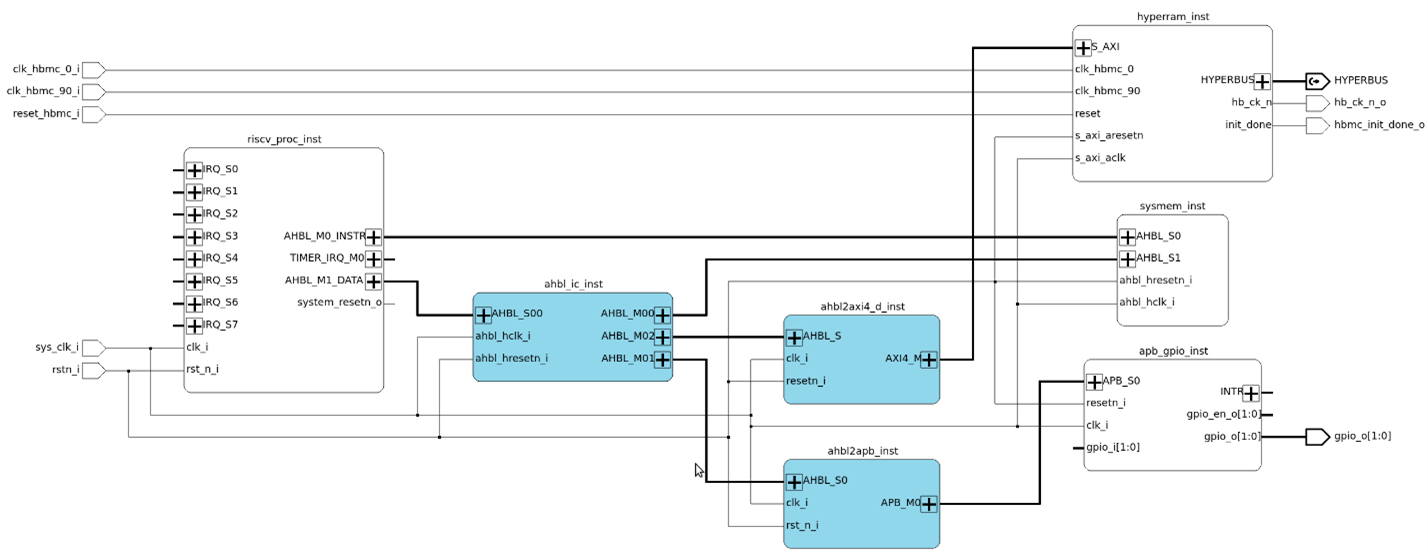
The block diagram illustrates the connections between the different IP blocks. First, the AXI slave controller will parse the user request. The information will flow to the HyperBus™ controllers by means of two FIFOs that act as frame buffers in case of congestion. The HyperBus™ controller contains the required logic to perform the operations over the memory. There are two FIFOs to perform the clock domain crossing between AXI and HyperBus™.
In HyperBus™ clock domain, there is the data recovery unit, which synchronizes the received data from the physical pins. Finally, the io buffers, that instantiate the buffers and the required delays to the signals


