Your first DSP module with Vitis HLS
Getting Started with Vitis HLS 2021.2
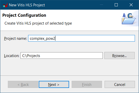
Create new Vitis HLS Project
- Open Vitis HLS 2021.2
- File > New project. Specify the project name and the location.
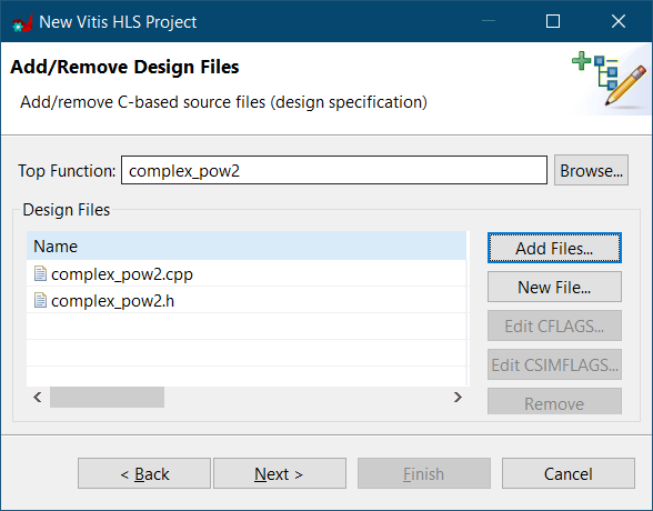
3. Add the top function name and the design files. The top function name represents the name of the function that we desire to implement in hardware. The design files are the files which contains the code (both declaration and definition) of the function.
4. Create a new testbench file. Adding ‘_tb‘ to the name of the file will clearly identify that this file contains the simulation code. This is a very standard way to visually separate files which contain simulation code from those that contain the implementation itself.

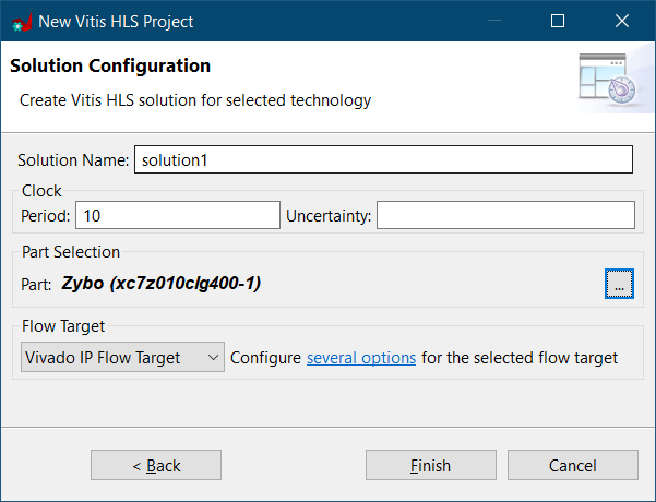
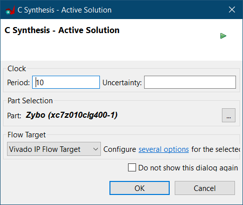
5. Configure your solution. A solution in HLS represents a particular implementation of the C/C++ code that we just added. Implementations vary in different aspects, for instance, the clock frequency or the part selection.
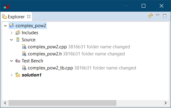
6. Finally, check under the Explorer window that both the design files and the testbench were successfully added to the project.
Modifying the Design Files and the Testbench
Design Files
The design files are files which contain C/C++ source code. The primary extension of these files are .c for C code and .cpp for C++. Includes which contain the declaration are also possible (extension .h). You can add multiple design files to your project but for the sake of simplicity, we added just one design file (complex_pow2.cpp) with its declaration (complex_pow2.h). Note that in the case that you have multiple design files, just one must be defined at the top-level function. You cannot define multiple top-level functions at the same time but you can select which top-function you want to synthesize at a given moment.
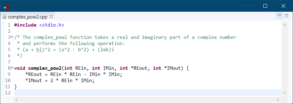
The design file has a main purpose: define very precisely the functionality of our function to be synthesized. As stated in the beginning of the blog-post, our functionality is based in the computation of the power of 2 of a complex number:
(a+bi)^2 = a^2 + (bi)^2 + 2abi = (a^2 - b^2) + (2ab)i
Therefore, given the real (a) and imaginary (b) part of a complex number, the output real and imaginary result must be:
RE = a^2 - b^2
IM = 2ab
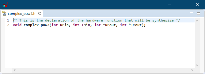
- REin and IMin are the real and imaginary part respectively of the input complex number. These arguments represent the inputs of our module.
- REout and IMout are the real and imaginary part respectively of the output complex number. These arguments represent the outputs of our module. Call by reference (argument pointers) is used to be able to return more than one variable in the function.
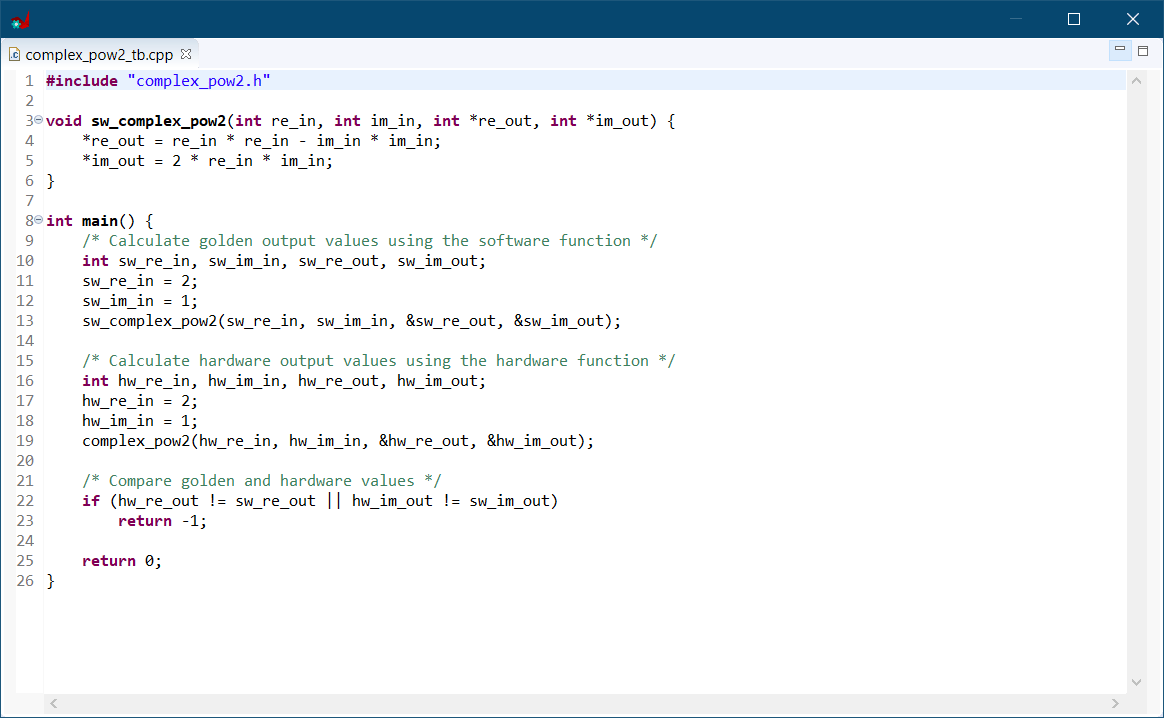
Testbench
In the previous step, we wrote the C/C++ code that we think it describes the intended functionality. But, are we 100% percent that it is correct? Well, the testbench will definitely solve our doubts!
The main idea behind a testbench is compare two sets of data:
- A set of data that we are 100% sure it is correct. It can be either golden values or the values generated from a software reference model. In this example, we decided to create a software reference model because its simplicity. With more complex designs another approach could be generate golden values using other tools such as MATLAB or Octave. The software reference model represents the “software” version of our hardware function and it will generate the correct values. It means, the values that properly represent the intended functionality of our design. The software reference model has been called sw_complex_pow2().
- A set of data generated by our hardware function – complex_pow2(). This values are the ones generated by the top-level function.
Our testbench is divided in three main parts:
- Calculate the output values using the software reference model.
- Calculate the hardware output values using the hardware function.
- Compare both values and check if they are the same.
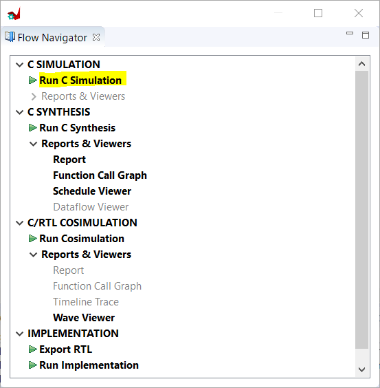
Run C Simulation
The C simulation is the first step in the Vitis HLS flow. This step takes the C/C++ source code of your testbench and it will compile, link and execute it. Therefore, it will check if the code is successfully builded and if the functionality implemented is the one intended at the beginning.
To execute this step, click in the following button inside the Flow Navigator window:
After completion, a log file is generated which contains the output from the C Simulation:
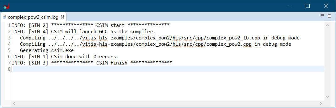
The complex_pow2_csim.log shows the output generated from the C Simulation. The compiler used for the simulation is GCC. An executable file (csim.exe) was generated from the result of the build process. After running the executable, we can check that it has finished successfully.
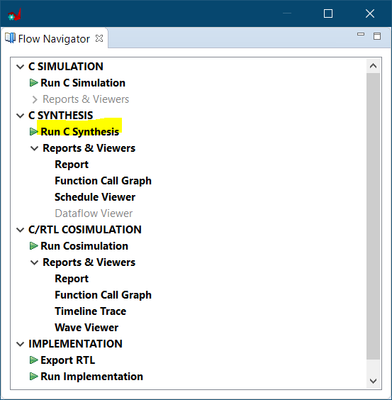
Run C Synthesis
After the synthesis has been completed, there are multiple hardware-related information available. For instance, timing estimation, performance and resource usage:
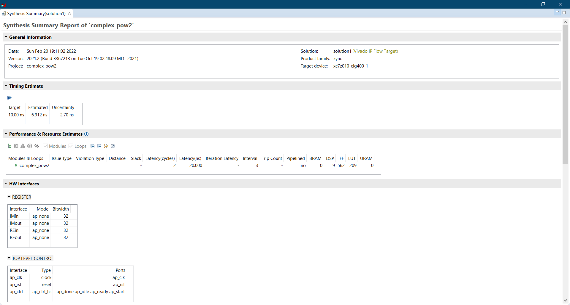
Timing Estimate
The active solution was configured to run at 100 MHz which represents the target frequency. However, the tool was able to achieve an estimated clock frequency of 144 MHz. The clock uncertainty was automatically set by the tool because we did not specified any value in the configuration. The clock uncertainty is the margin used by the tool for other processes like place and route. Note that if the estimated clock frequency plus the clock uncertainty are greater than the target frequency, then a timing violation is issued.
Performance & Resources Estimates
This is the section where we can see clearly that the operations performed in our C/C++ code are mapped into hardware resources of our target FPGA. This mapping will depend on multiple factors, for instance:
- How our code is written.
- Pragmas used.
- Target platform.
From the report we can check that in our case the resources used are:
- 0 BRAM
- 9 DSP
- 562 Flip-flops
- 209 LUT
- 0 URAM
In addition to the hardware resources used, there are more information that can be extracted. For instance, if the function has been pipelined, the throughput (interval) and the latency.
HW Interfaces
The HW interfaces were mapped as:
- Two 32-bit data input ports (REin, IMin),
- Two 32-bit data output ports (REout, IMout).
The are additional interfaces that are needed to run the hardware module. Those interfaces are ap_clk and ap_rst which represent the clock and the reset of the module respectively.
There is an additional interface (ap_ctrl) added also automatically by the tool and it is the default top level protocol for the return port of our function.
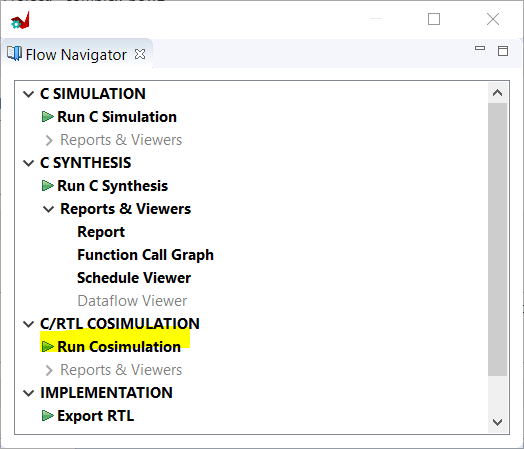
Run Co-simulation
The C/RTL Co-simulation will compare both the software implementation (C Simulation step) and the hardware implementation (C Synthesis step) and it will check if the same results are achieved. In this way, the tool can check that the synthesis of the function was properly done and its results are the same as the software reference model.
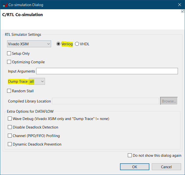
In the C/RTL Co-simulation window, select Vivado XSIM as RTL simulator. Select Verilog to have access to the full features of Vitis HLS. If you select VHDL, you will not have access to some of them, for instance, the wave viewer or the timeline trace.
Select Dump Trace “all” to activate the wave viewer. This will record all the signals in our design to be able to visualize them after co-simulation.
The extra options are quite interesting when using the DATAFLOW pragma. In our case, we left them unchecked.
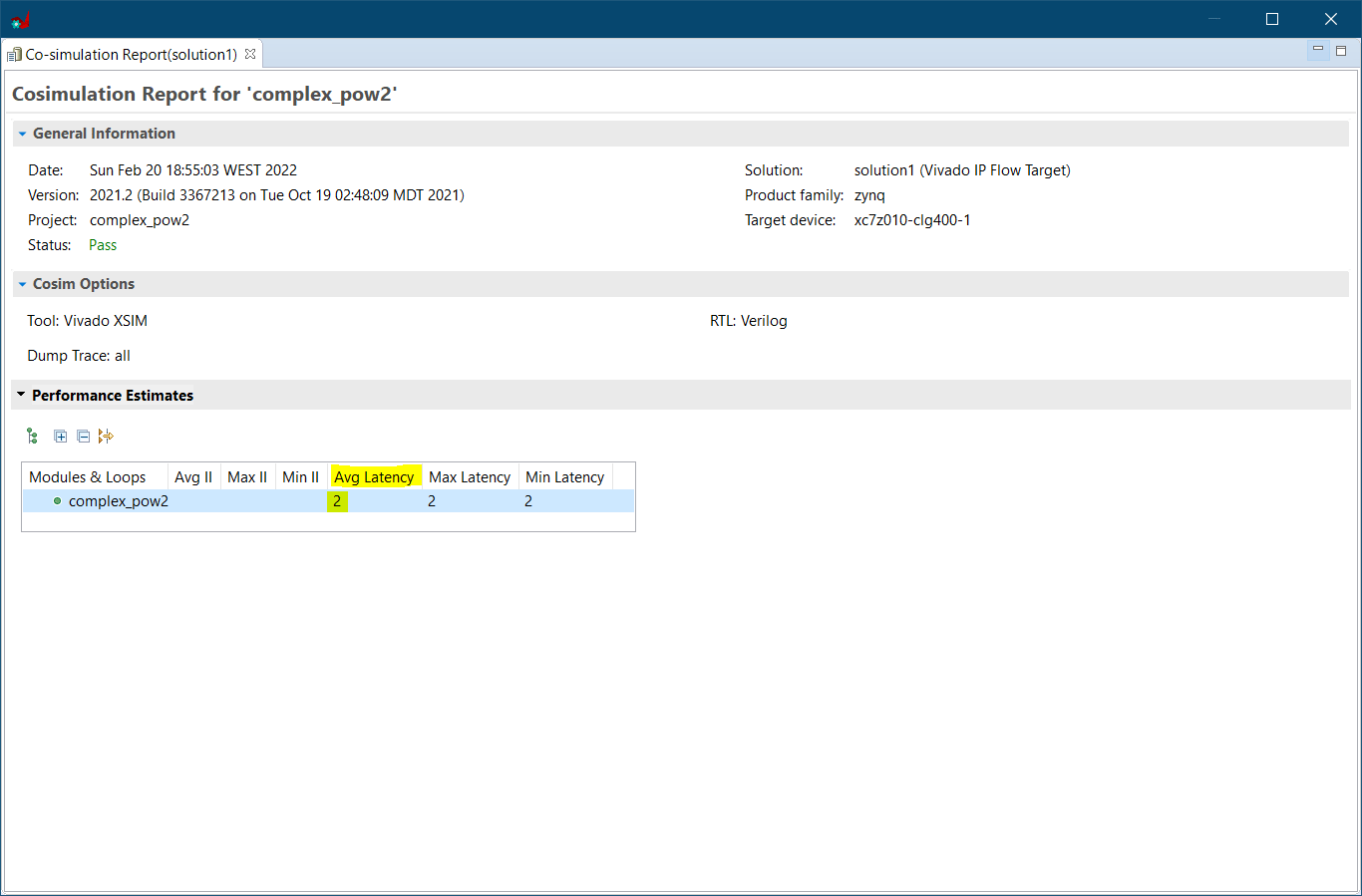
The Co-simulation has been successfully completed. A new report is available, showing some performance estimations. The latency of our module is 2, which means the number of clock cycles that our module needs to complete its operations since a new input was feed.
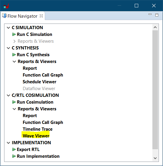
A waveform is also available. Click in Wave Viewer under the C/RTL Simulation field.
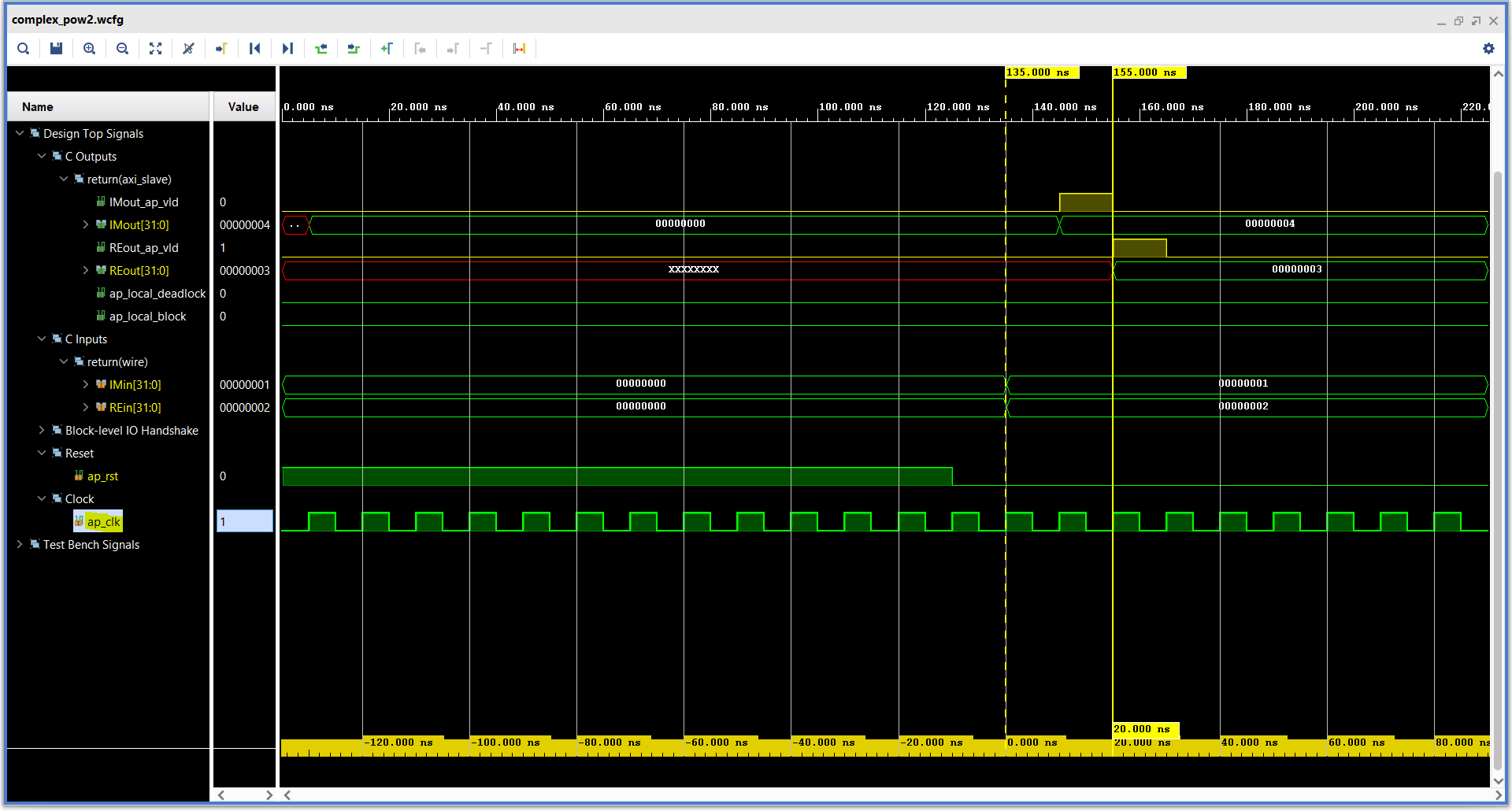
The inputs of our design, REin and IMin, are set at the same time to 0x2 and 0x1 respectively. Then, after one clock cycle, the imaginary part (IMout) is available but the real part (REout) is available two clock cycles after. The operations performed in the IMout and REout are not the same and the way the tool schedules them will determine its latency.
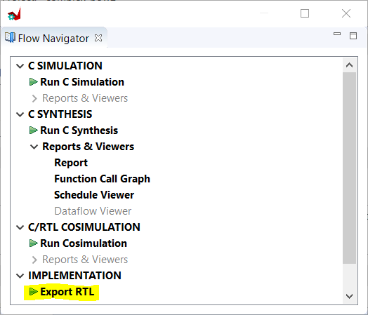
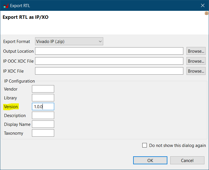
Export RTL
Exporting the RTL design is the final step in the Vitis HLS flow. This will package the module into a .zip to be used as an IP. You can configure some parameters of this IP such as vendor, version and description: